-40%
Band decoder sequenser protection for amplifier SD2933 MRF150 BLF188 BLF578
$ 49.63
- Description
- Size Guide
Description
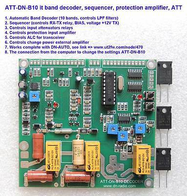
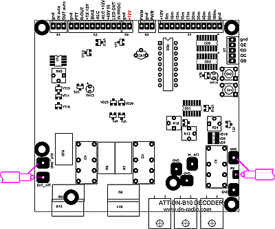
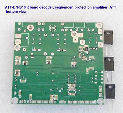
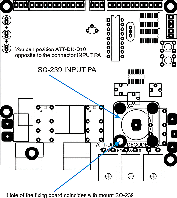
This deviceATT-DN-B10
is a further development of the board
DN-B10
. The detailed description of the board
DN-B10
you can see by the link => dn-radio.com
Possibilities demonstration of, see - YouTube -
UT2FW
link =>
youtube.com/watch?v=lz3VUaQwwsk
The device
ATT-DN-B10
includes such functions:
1. Automatic
Band Decoder
(10 bands, controls LPF filters)
2.
Sequencer
(controls RX-TX relay, BIAS, voltage +12V TX)
3. Controls input
attenuators relays
4. Controls
protection input amplifier
5. Controls
ALC
for transceiver
6. Controls
change power
external amplifier
7. Works complete with
DN-AUTO
, see link =>
dn-radio.com
8. The connection from the
computer
to change the settings ATT-DN-B10
It can be used to automatically select any devices in accordance with the frequency of the signal applied to the Band Decoder. For example, to switch antennas, filters, amplifiers.
The principle of operation of the Band Decoder based on the measuring the frequency of the signal from the transmitter. (Automatic band change based on TX frequency.)
It is sufficiently high frequency voltage from ~5V for stable operation, which corresponds to the power of 0.5 W at impedance of 50Ohm.
The control of the Band Decoder performs the microprocessor PIC16F648A. The cymometer of the microprocessor determines the frequency of the input signal and sets the appropriate range. The minimum tuning step of frequency is 10kHz. Border ranges are distributed as follows:
1.0 – 2.5MHz – 160m;
2.51 – 4.0MHz – 80m;
4.01 – 8.0MHz – 40m;
8.01 – 11.0MHz – 30m;
11.01 – 16.0MHz – 20m;
16.01 – 20.0MHz – 17m;
20.01 – 23.0MHz – 15m;
23.01 – 26.0MHz – 12m;
26.01 – 31.0MHz – 10m;
31.01 – 55MHz – 6m;
The Sequencer controls the operation mode switching RX-TX amplifier. For safe switching is observed a certain sequence of control signals. The algorithm was written in the program of the microprocessor.
The order of the amplifier from the RX-mode to the TX-mode is as follows:
1.The Band Decoder turns on corresponding range filter in the amplifier.
2.It is measured the input power. If the input power exceeds the power recorded in the memory of the microprocessor – it prohibits the next step and stops the work. The indicator LCD board DN-AUTO CPU is blinking in this case.
If the power does not exceed the power recorded in the memory of the microprocessor – it allows the next step – turning on the Sequencer.
The Sequencer is turning on from the PTT signal from the transceiver.
3.ALC reduces the power of the transceiver to 0W at 50mS.
4.During 50mS while ALC is turned on, the antenna is connected to the output of the amplifier. The delay of the antenna relay is 40mS.
5.The amplifier input is connected to the transceiver. The delay of the relay is 10mS.
6.The voltage BIAS is served .
7.ALC increases the power of the transceiver to the nominal.
8.When the transceiver is returned to RX-mode the Sequencer is turning off and the amplifier is switching to the RX-mode.
A description of work the ATT-DN-B10.
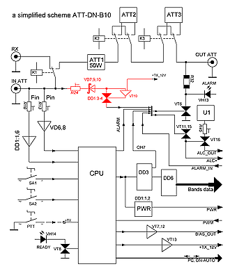
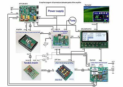
The simplified circuit diagram of the board shown in
Figure 1
.
A detailed circuit diagram provided to the board on the enclosed CD.
Designations of components in the simplified circuit diagram correspond to the designations of the components on the detailed circuit diagram on CD.
The signal from the transceiver supplied to the IN-ATT input. The relay K1 switches the input of the amplifier.
The RX output supplied to the relay, which switches the output of the amplifier (it is a so-called "bypass" of the amplifier).
As a result, in the RX mode the transceiver has connected to the antenna through the contacts IN-ATT – K1 – RX – the power relays of the amplifier output.
When switching the amplifier into the TX mode (the contact PTT is connected to GND) – the input IN-ATT connects to the input of the amplifier through contacts of the relay K1.
The ATT1 with attenuation of 6 dB installed on the input of the board. The ATT1 includes powerful resistors, each on 30W. The ATT1 can withstand up to 100W for a short time. The rated power of the ATT1 is 50W.
Then two more attenuators (ATT2, ATT3) turned on consistently through contacts of the relays K2, K3. You can choose of the four state attenuators at any band:
1.Both ATT off.
2.Turns on ATT No. 1.
3.Turns on ATT No. 2.
4.Turn on both ATT.
State of attenuators are selected on the stage of programming the microprocessor CPU.
In the original program to turn on used next an algorithm:
160m, 80m, 40m, 30m - ATT1 on, ATT2 off.
20m, 17m, 15m, 12m, 10m - ATT2 on, ATT1 off.
6m - both ATT1-ATT2 off.
A powerful shunting resistor R32 makes a protection of the amplifier input.
The protection is fast acting, because the key to MOSFET VT6 provides the connection R32. A voltage of +48V securely holds closed key VT6 to avoid its opening by input power.
The LED VH13 ALARM indicates when the protection turned on.
There are two automatic circuit for monitoring an overload and turning on the R32. The first circuit is analog it is highlighted on the circuit diagram by red components. The second circuit is digitally on the microprocessor CPU.
Resistors R13, R24 are set the upper threshold power for turning on the protection.
Both protection circuit have the "latch". You cannot disable the protection after turning on when the power has reduced until the amplifier has not returned in the RX mode. Thus, if the protection has tripped, you need to switch from TX mode to RX mode.
The protection turned on in the circuit QH7 for the time of switching relays RX-TX – 50ms.
The circuit ALARM_IN performs external control of the protection turning on. For example, by the signal from the comparator SWR-meter of the Out Unit board.
Other functions of the ATT-DN-B10 board correspond to the functions of the DN-B10 board. You can get more details about the DN-B10 by the link => ut2fw.com
Therefore, I will try to speak briefly about them here.
U1, VT16, VT11, 15 provide control signals to the ALC transceiver: the ALC_OUT is a voltage of negative polarity and the ALC+ is a voltage of positive polarity. You can adjust the voltage ALC_OUT (from 0V to -9V) by the resistor R45.
The decoder DD6 controls selection on the 10 bands.
The compliance bands and frequencies described further in the text.
The Decoder/Driver 74LS145D is using as the DD6. The manufacturer of the 74LS145D announce this Decoder/Driver as switching a relay. The quote from the dataset on 74LS145D: «It is designed for use as indicator/relay drivers or as an open-collector logic circuit driver». However, it is not specified anywhere in the description about availability of protective diodes for keys 74LS145D. The performance of the 74LS145D for control of relays in LPF600, LPF1200, and LPF1500 had checked without additional protective diodes. I recommend using shunting of the relay winding with an additional diode to increase reliability.
The PWR signal can be using as a reference voltage to control of the power and protection of the transceiver and amplifier. Read more about this feature further in the text.
The PWM signal disables the operation of DD6, i.e. the Bands Decoder.
BIAS_OUT is the BIAS voltage for the amplifier.
+TX_12V is the +12V TX voltage.
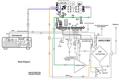
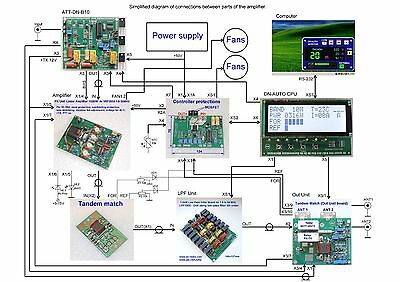
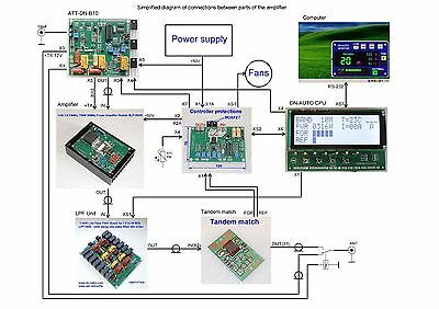
PC, DN-AUTO – The board ATT-DN-B10 can be using in the DN-AUTO complex. The complex DN-AUTO of the three boards: DN-AUTO CPU, Controller Protections, ATT-DN-B10 provides full control of the amplifier protection, output an information on the LCD display, on the monitor of the computer (a program has developed the AmpMonitor for computer),
control of the LPF, antennas and many other features. The detailed description of the DN-AUTO you can read by the link => dn-radio.com
The ATT-DN-B10 is able to connect to COM-port of the computer via additional RS232. The computer program, which allows changing CPU settings, has developed.
The VH14 LED indicates the presence and capture of the input frequency by the CPU frequency meter.
Settings of voltage levels of the PWR and input power are changing by the buttons SA1, SA2. These levels are set and stored in the CPU separately for each band. Therefore, you can always adjust the protection (power) settings individually to your amplifier for each band separately.
The resistor R10 adjusts the sensitivity of the CPU frequency meter. The initial setting is on 10W.
A detailed description of the settings ATT-DN-B10 are enclosed on CD to the board.
Applying of the ATT-DN-B10
The supply voltage for the board is stabilized +12-13V. The current is up to 100mA.
The control signals of the ATT-DN-B10 are output to the
connector X3
.
Pin #1
. The ALARM_IN input is an external signal that turns on the protection of +10-12V.
Pin #2
. The LED output for additional LED indicating when the protection is turning on. You can place this LED on the front panel of the amplifier. To the anode of the LED to feed from +5V to +12V.
Pin #3
. The voltage +48-60V supplied from the power supply of the amplifier. This is an additional locking voltage for the VT6 key. It is not necessary to apply this, because the VT6 has not a significant impact on the input signal of the amplifier. Supply the +48-60V voltage can be useful for a large input power on the 6m band.
Pin #4
. The output ALC+12V – power voltage +12V, up to 100mA. Its function is similar to ALC, but it is another type of output (outgoing) signal. The ALC+12V signal appears only when is the PTT signal and the Sequencer is turned on. The duration of the ALC+12V signal is 50mS since turning on the Sequencer. The Appendix contains the schemes of applying ALC+12V.
Pin #5
. The output ALC is the сontrols of ALC of the transceiver. The voltage can be adjusted by trimmer R36 from 0V to -9V, current up to 10mA. The ALC signal appears only when is the PTT signal and the Sequencer is (activated) turned on. The duration of the ALC signal is 50mS since turning on the Sequencer.
Pin #6
. The BIAS output – the voltage of +12V to 100mA. It is the bias voltage for the transistors of the amplifier. The voltage of the BIAS appears after 50mS from R-OUT signal and 10mS from the R-IN signal. Time delays can switch reliably the R-OUT and R-IN relays. Thereby the accident of amplifier is eliminating.
Pin #7
. The output +TX 12V – the voltage of +12V, up to 100mA. The voltage TX +12V is designed for switching circuits of the amplifier to transmission mode. The voltage appears when you press PTT if the Sequencer is turned on.
Pin #8
. The R-OUT output – TTL +5V, up to 10mA. The control of the antenna relay is in the amplifier. It is formed when is the presence of a PTT signal if the Sequenceris (activated) turned on.
Pin #9
. The PTT input. It must be shorted to ground. It is the control of the Sequencer. The +TX 12V; ALC +12V; ALC +S; ALC; R-OUT signals will appear first if not exceeded the threshold of input power P; Through 40mS appears R-IN, then after 10mS appears BIAS and ALC +12V; ALC +S; ALC will turn off. When you turn off PTT the Sequencer is deactivated and all the signals will turn off.
Pin #10
. The ground GND. Connect the negative supply voltage.
The X2 Connector
.
Binary-decimal codes to control additional decoders, similar to the DD6, are output to this connector. In fact, this is duplication of the DD6 decoder. Why has it done for? In some cases, easier to lead five control wires to dial-up devices and the 74LS145 next to it, than to lead 12 wires from the X1 connector. If wires from the X2 connector to the performing device will be long, you should place them into a screen or use ferrite clips.
The X4 Connector
.
Connects the ATT-DN-B10 with the DN-AUTO CPU board or via additional RS232 serial converter with computer.
There are two versions of the program for the CPU ATT-DN-B10. The first program provides an additional comparison of the band, which the frequency meter of the CPU of the ATT-DN-B10 board has determined, with the band determined by the CPU of the DN-AUTO CPU board. Remember that the DN-AUTO CPU gets data about the band from the transceiver. If these bands do not coincide then the DN-AUTO CPU will go to the accident mode and the Sequencer of the ATT-DN-B10 board will not turn the amplifier to the TX mode. Thus, an emergency when a band of the transceiver do not coincide with a band of the amplifier eliminated.
It should be noted that the ATT-DN-B10 specifies 10 bands in the frequency band of 1-55MHz. The bands of 17m, 12m, and 6m have excluded from the data of ICOM Band voltage output band of ICOM transceivers. The ICOM Band voltage output combines bands of 17/15m, 12/10m and does not provide information about inclusion of 6m. Therefore, the DN-AUTO CPU board will turn on an "accident" on the bands 17m, 12m, and 6m when using the ICOM Band voltage output to determine the band. You need to use port CI-V ICOM when using of a program providing an additional comparison of bands in the CPU ATT-DN-B10. The CI-V ICOM port gives information about all 10 bands. Therefore, the work of the ATT-DN-B10 together with the DN-AUTO will be correct.
The second program for the CPU of the ATT-DN-B10 board has not additional bands comparison, so it can be using with the ICOM Band voltage output.
By default the ATT-DN-B10 board (DN-AUTO complex) is equipped the CPU with a comparison program. Because this option has the highest degree of protection for the amplifier. If you must use the ICOM Band voltage output, then ask for the ATT-DN-B10 equipment without bands comparison.
The ATT-DN-B10 board lost the display that was in the previous DN-B10 board. Therefore, a computer program the Remote Control PA for configuring of the ATT-DN-B10 has developed, which displays all the settings of the CPU.
You need a RS232 serial adapter to connect the ATT-DN-B10 to the COM port of a computer. You can buy a ready adapter there are many offers for sale on the Internet. Alternatively, you can make such an adapter yourself. A possible scheme of the RS232 has given in the Appendix.
The X5 Connector.
Pin #1
. The PWR input. It turns off DD6 74LS145D when applying + 5V. You can turn off the control DD6 by activation of the PWR if the amplifier provides additional control of the LPF relay from the switch or the transceiver.
Pin #2
. The ground GND. Connect the negative supply voltage.
Pin #3
. The PWM output. The voltage of this output can be programmed from 0V to +5V. The load resistance for voltage of PWM should be at least 10k.
You need to enter the menu to set the voltage level. Before turning on the Band Decoder press and hold the button SA1. Turn on the Band Decoder. Set the desired voltage level by buttons. Press simultaneously both buttons to save the value. The voltage is stored individually for each range, in ten separate memory cells. Now when turn on the voltage range the PWM will be restored to level stored in memory of the microprocessor. The Appendix contains the schemes of possible application the voltage of PWM in the protection of the amplifier.
The limit voltage of the input frequency Fin ~5V to ~70V. The optimum value of the voltage ~15V to ~30V. The sensitivity of the Fin input is adjustable with variable resistor (trimmer) R10. The sensitivity of the Fin input sets on a stable working of the cymometer on all bands. To adjust the sensitivity of the Fin should be at smaller power values. To start the adjustment in position of the rolling contact R10 closer to the output connected with ground. Frequency is served to connector IN_ATT – IN_GND.
The sensitivity of the input of the input power meter Pin is adjusted by a variable resistor (trimmer) R13.
For control of the Low Pass Filters relay is used DD6 74LS145D. The limiting parameters of one key of this chip are the current up to 80mA, the voltage up to 15V. Key – transistor with open collector. The LPF relay must be diode device is activated from the surge reverse current. The outputs the keys of the chip output to the X1connector.
The measured input power – Pin is the special feature of DN-B10 and ATT_DN-B10. The power values P are stored in 10 memory cells of the microprocessor separately for each range. When the input power is exceeding the value stored in the memory cell is activated a ban on the next step of the program.
You need to enter the menu to set the voltage level. Before turning on the Band Decoder press and hold the button SA2. Turn on the Band Decoder (apply +12V). Set the desired voltage level by buttons. Press simultaneously both buttons to save the value. Now when you turn on each voltage range, the P will be restored to the level saved in the memory of the microprocessor.
It is desirable to set this level Pin to measure when the values of P will be close to the maximum value of 10-14. This minimizes the hazardous impact of inductions on the circuit of the power measurement.
As soon as the input power Pin exceeds the level P in the memory cell is activated ban program. Blinking of LCD DN-AUTO CPU and LED VH13 ALARM of the is indicated for the ban. Accordingly, the Sequencer doesn't turn on and the amplifier doesn't go to TX mode.
The ALC+12V, ALARM, ALC signals will appear and BIAS turns off if the value Pin exceeds the value P when the Sequencer is turned on. Thus the power of the transceiver will decrease and protection system (R32) will switch the amplifier to safe mode. The indicators of the range will blink and the operation of the Sequencer will be blocked until switch to the mode RX.
The pinout of connectors.
X1 Pinout
PIN
SIGNAL
DESCRIPTION
1
GND
Ground.
2
160m
Open collector 74LS145. Current up to 80mA, voltage up to 15V.
3
80m
Open collector 74LS145. Current up to 80mA, voltage up to 15V.
4
40m
Open collector 74LS145. Current up to 80mA, voltage up to 15V.
5
30m
Open collector 74LS145. Current up to 80mA, voltage up to 15V.
6
20m
Open collector 74LS145. Current up to 80mA, voltage up to 15V.
7
17m
Open collector 74LS145. Current up to 80mA, voltage up to 15V.
8
15m
Open collector 74LS145. Current up to 80mA, voltage up to 15V.
9
12m
Open collector 74LS145. Current up to 80mA, voltage up to 15V.
10
10m
Open collector 74LS145. Current up to 80mA, voltage up to 15V.
11
6m
Open collector 74LS145. Current up to 80mA, voltage up to 15V.
12
+12V
Output +12V. Connected in parallel to a contact +12V
X6
.
X2 Pinout
PIN
SIGNAL
DESCRIPTION
1
GND
Ground. Chassis ground.
2
QE
Connecting an external decoder 74LS145D – pin 12.
3
QD
Connecting an external decoder 74LS145D – pin 13.
4
QC
Connecting an external decoder 74LS145D – pin 14.
5
QB
Connecting an external decoder 74LS145D – pin 15.
X3 Pinout
PIN
SIGNAL
DESCRIPTION
1
IN_PROC
Input. Is an external signal of +10-12V, that turns on the protection.
2
LED_OUT
Output. LED Alarm protection on the front panel of the amplifier.
3
+48V IN
Input. The voltage +48-60V supplied from the power supply of the amplifier.
4
ALC+12V
Output +12V to 100mA. Control transmission power of the transceiver.
5
ALC
Control of ALC of the transceiver. Adjustable output from 0V to -9V, to 10mA.
6
BIAS
Output +12V to 100mA. The bias voltage for the transistors of the amplifier.
7
+TX 12V
Output +12V to 100mA. Voltage +12V TX.
8
R-OUT
Control of the OUT-relay. TTL output +5V up to 10mA.
9
PTT
PTT input. Shorted to ground for translation in the TX-mode.
10
GND
Ground.
X4 Pinout
PIN
SIGNAL
DESCRIPTION
1
OUT auto
To the IN board DN-AUTO CPU
2
IN auto
To the OUT board DN-AUTO CPU
3
GND
Ground. Power supply return. Chassis ground.
X5 Pinout
PIN
SIGNAL
DESCRIPTION
1
PWR
Input. Disables the control of the LPF relay. Apply +5V.
2
GND
Ground. Power supply return. Chassis ground.
3
PWM
Control of the protection, voltage from 0V to + 5V. The load current is less than 0,5mA. Rl > 10k.
X6 Pinout
PIN
SIGNAL
DESCRIPTION
1
+12V
The supply voltage from +12VDC to +14VDC. The current consumption 100mA.
2
GND
Ground. Power supply return. Chassis ground.
